Inside the 3D chip design that may unlock AI’s next leap: Stacking silicon vertically may decide the future of artificial intelligence
For more than a decade, the artificial intelligence industry has measured progress in familiar units: faster GPUs, larger models, more parameters, more compute. But as AI systems scale, something unexpected is happening. Performance limits are no longer showing up where engineers assumed they would.
In many modern AI workloads, compute is available. Models are optimized. Yet systems still slow down. Power ceilings are hit before theoretical throughput. Cooling systems strain. And beneath all of it lies a quieter, more stubborn constraint: the cost of moving data.
Inside today’s chips, performance is increasingly governed not by how fast calculations can be performed, but by how quickly information can travel between memory and compute. That friction, measured in nanoseconds and joules, is becoming the defining bottleneck of the AI era.
The question now confronting hardware designers is deceptively simple: if distance inside a chip is the problem, what happens if we eliminate distance itself?
The Memory Wall Nobody Can Ignore
For years, researchers have warned about the so-called “memory wall”, the growing gap between compute speed and memory access. As AI models balloon in size, they require constant movement of weights, activations, and intermediate results. That movement is expensive.
Traditional chips are flat. Memory and logic sit side by side, connected by a limited number of shared pathways. As workloads grow, those pathways become congested. Operations that could run in parallel are forced to wait their turn. Compute units idle. Energy is wasted shuttling bits across silicon highways that were never designed for this scale.
The result is a paradox: even as chips grow more powerful, real-world utilization drops. More transistors do not automatically translate into more intelligence.
This is no longer a theoretical concern. It is now one of the primary constraints shaping AI system performance.
Rethinking Silicon in Three Dimensions
A new study from researchers at Stanford University, Carnegie Mellon University, the University of Pennsylvania, and MIT suggests that the solution may lie not in faster processors, but in a radical rethinking of chip architecture itself.
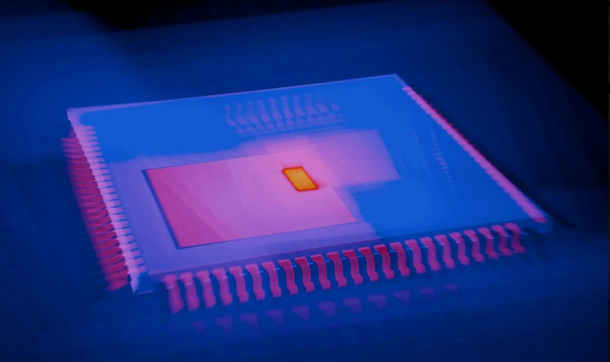
Working with SkyWater Technology, a commercial semiconductor foundry, the team developed a monolithic 3D chip, an architecture in which memory and logic are stacked vertically rather than spread across a flat surface.
The difference is profound.
By stacking components, the chip replaces long, shared internal data paths with dense networks of short vertical connections. Data no longer needs to traverse wide horizontal distances. It moves directly between layers, faster and with far less energy.
In early tests, the prototype outperformed comparable conventional chips by several multiples. In simulations that scale the design upward, the gains grow even larger, particularly for AI workloads dominated by frequent memory access.
The implication is clear: reorganizing silicon around data locality does not just optimize performance at the margins. It changes how AI workloads execute at a fundamental level.
Why This Matters More Than Faster GPUs
The AI industry has become accustomed to performance gains delivered by brute force: larger clusters, higher wattage, denser racks. But those strategies are colliding with physical and economic limits.
Power grids are strained. Data centers face cooling constraints. Energy costs are rising. In this environment, efficiency is no longer a secondary concern, it is existential.
What the Stanford-led research demonstrates is that internal data movement is now a first-order design problem. No amount of additional compute can overcome a bottleneck created by serialized memory access and long-distance data transfers inside a chip.
By shortening those paths, monolithic 3D architectures improve both speed and energy efficiency. Less energy is spent moving information. More time is spent computing.
This matters not just for performance benchmarks, but for the viability of large-scale AI itself.
From Lab Curiosity to Infrastructure Capability
Three-dimensional chip designs are not new. Researchers have explored them for years. What has been missing is proof that they can be fabricated reliably in a commercial environment — not just as lab demos, but as repeatable, scalable products.
That is what makes this work different.
By building the chip with an established foundry, the researchers have shown that vertical integration can move beyond experimental novelty and become an infrastructure capability. This opens the door to faster iteration cycles, broader participation, and real-world deployment.
“This opens the door to a new era of chip production and innovation,” said Subhasish Mitra of Stanford, a principal investigator on the project. His claim that future AI systems will demand thousand-fold hardware improvements may sound bold, but it reflects a growing consensus: incremental gains will no longer be enough.
The Challenges Are Real and Unavoidable
None of this comes without trade-offs.
Stacking silicon vertically introduces serious challenges in thermal management. Heat becomes harder to dissipate as layers multiply. Manufacturing yield becomes more complex. Design complexity rises sharply as interactions between layers must be carefully modeled and validated.
Software, too, must adapt. Hardware gains will only be fully realized if compilers, runtimes, and AI frameworks are designed to exploit vertical locality.
But these are not reasons to dismiss the approach. They are signs that hardware innovation has entered a new phase, one where architecture, fabrication, and software must co-evolve.
As H.-S. Philip Wong of Stanford noted, the significance of this work is not just performance, but capability. The ability to build advanced 3D chips expands the design space itself.
A Shift in How AI Progress Is Measured
For years, AI progress has been framed as a race for scale: bigger models, bigger clusters, bigger budgets. But the physics of silicon is forcing a recalibration.
The next phase of AI will be defined less by raw compute and more by how intelligently systems move data. Efficiency, locality, and architectural innovation will matter as much as transistor counts.
Monolithic 3D chips do not eliminate the memory wall entirely. But they show that it is not immutable. Distance inside silicon is a design choice, and one that can be changed.
If the AI revolution is to continue without collapsing under its own energy and infrastructure demands, breakthroughs like this will not be optional. They will be foundational.